Instruments and Capabilities
The combination of the Electron Microprobe and Scanning Electron Microscope allows for a number of applications and specializations for a diverse range of fields of study. We list just a few of the projects that we have or are currently working on:- Archeology: Mineral chemistry and mineral phase analysis of potsherds to determine material source location.
- Environmental Geology: Analysis of uranium mining waste from many decades ago, now contaminating aquifers in New Mexico and Arizona.
- Planetary Science:
- Ongoing characterization of new meteorite finds.
- High-resolution imaging and X-ray mapping of Martian meteorite NWA 7034 (Black Beauty).
- Analysis of Lunar sample 73002, a "drive tube" core sample, opened for the first time 40 years after being collected by Apollo 17 astronauts
- Industry: High-resolution surface imaging for the determination of the effects of Particle Beam bombardment.
- Biology: Exploration for evidence of microbial life in caves as analogs for the search for life on other planets.
- Chemistry: Chemical analysis of vapor-deposited thin films.
- Medicine: Imaging and chemical analysis of potentially toxic microplastics.
- Engineering: Imaging of filtered particulates in a new generation of water purification for third-world countries.
Instrumentation:
JEOL 8200 Electron Probe Microanalyzer
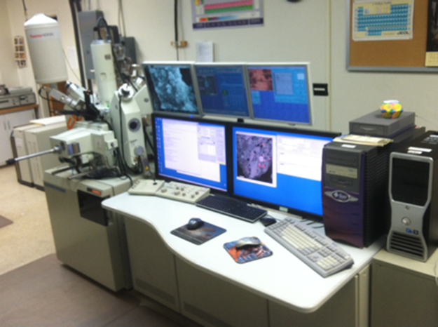
The Electron Microprobe (EMP) laboratory houses a JEOL 8200 microprobe, installed in Spring 2003. The probe is equipped with 5 wavelength-dispersive (WD) spectrometers and an ultrathin-window energy dispersive spectrometer. The WD spectrometers are fitted with multiple analyzing crystals to provide quantitative analysis of all elements from Be to U. Two spectrometers are high-sensitivity detectors, and one spectrometer has a large PET crystal suitable for precise measurement of Pb, Th, and U at low concentrations. In addition, a LaB6 gun provides superior spot resolution for imaging and analysis of small particles. Instrument vacuum is achieved using a turbomolecular pump backed by a scroll pump, and thus, the system is completely dry-pumped to reduce contamination during long analyses, making it an ideal system for both major and trace element investigation and analysis of light elements. A powerful Sun Blade 2000 graphics workstation controls the fully automated system and can provide high-resolution and high-sensitivity X-ray maps over entire thin sections in order to find small, widely scattered analysis targets.
Tescan Vega 3 Scanning Electron Microscope
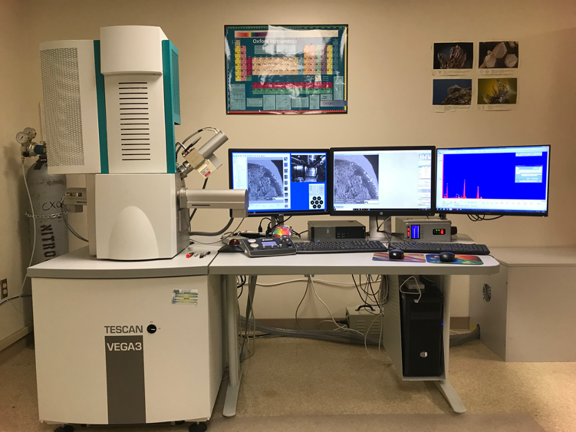
The scanning electron microscope laboratory (SEM) contains a new Tescan Vega3 XMU scanning electron microscope (Tescan Orsay Holding a.s., Brno, Czech Republic). The instrument is equipped with a LaB6 electron gun for high-resolution imaging. An extra-large sample chamber can accommodate specimens up to 6 inches (15.2 cm) across and has 5 motorized axes to provide fully automated stage movement. The SEM employs secondary electron (SE), low-energy backscattered electron (BSE), and 4-channel color cathodoluminscence (CL) imaging detectors. The instrument utilizes an IXRF silicon drift detector for energy dispersive /x-ray spectroscopy (EDS) (IXRF Systems, Austin, Texas) with Iridium Ultra software to analyze elements from boron and above. The SEM is a "dual mode” microscope that can operate at both high vacuum (the conventional mode of operation) and low vacuum, utilizing either the BSE detector or the specially designed low vacuum Tescan SE detector. Full stage automation is also supported by the IXRF system to allow the collection of large-scale EDS X-ray maps.
